SK Hynix invests 54 trillion KRW to build the Y2 wafer fab in Yongin and the M17 wafer fab in Chungcheongnam-do
2026-08-07
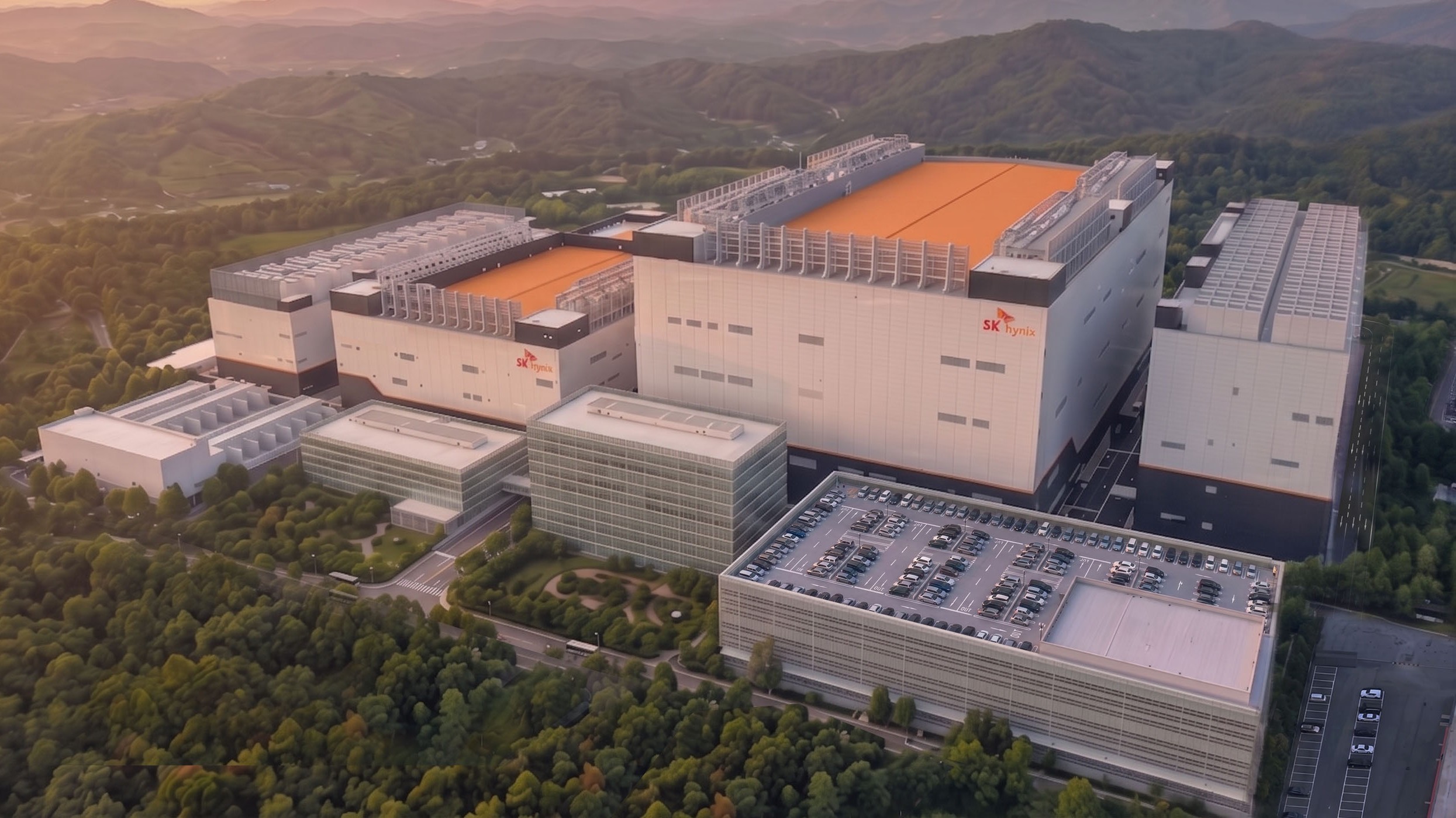
On August 7, 2026, SK Hynix announced that the company will build new wafer fabs (Fab) in Longin and Cheongju, South Korea to meet the growing memory demand in the AI era.
On the same day, the company's board of directors passed a resolution to invest 35.2 trillion Korean won and 19.1 trillion Korean won respectively in the construction projects of Longin "Y2" and Cheongju "M17" wafer fabs, with a total investment of approximately 54 trillion Korean won.
This move is another key progress in implementing the company's medium - and long-term investment strategy announced in June this year. Previously, SK Hynix announced plans to invest KRW 60 trillion in the Longin Semiconductor Cluster and KRW 100 trillion in the expansion of the Cheongju production base. At present, the construction of Longren's first wafer fab (Y1) is progressing in an orderly manner, and this investment decision marks the start of subsequent wafer fab construction in both Longren and Qingzhou.
SK Hynix stated, "In the era of AI, technological competitiveness alone is no longer sufficient to maintain an advantage; The true competitiveness lies in delivering sufficient products at the time required by customers. This investment decision was made based on a thorough assessment of market demand. ”
Longren Y2 is the second of four wafer fabs constructed by the company within the Longren semiconductor cluster, with a total construction area of approximately 341000 square meters (approximately 1.13 million square meters), and will be put into operation as a DRAM production base. The project is scheduled to start construction in July next year and the first clean room will be put into use in June 2029, mainly producing new generation DRAM products such as HBM. At present, the construction of Y1 wafer factory is progressing smoothly, and the first clean room is expected to be put into use in February next year.
Previously, SK Hynix had significantly advanced the overall completion time of the Longin Semiconductor Cluster from the original 2045 to 2033, completing the construction of all four wafer fabs. The Y2 construction this time is a key measure in the second phase to support this goal, and the investment will be implemented in stages until October 2031.
The investment amount also includes the construction costs of the office and welfare facilities "Support Building" for Y2 employees, the "R&D Comprehensive Center" integrating product development experiments, testing, and analysis, as well as related supporting facilities *.
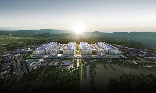
The Longin Semiconductor Cluster is located in the far three sides of Chuin gu, Longin City, Gyeonggi Province, South Korea, covering an area of approximately 1.26 million ping (approximately 4.16 million square meters). At present, the first phase of power and water supply infrastructure construction supporting Y2 production has been completed by 99% and entered the final stage. The company's goal is to synchronize the construction of wafer fabs and infrastructure, and Y2 will steadily advance according to the original plan to ensure that the project schedule is not affected.
With the accelerated popularization of AI services, the demand for NAND flash memory is rapidly growing, with enterprise solid state drives (eSSD) as the core. At the same time, the demand for KV cache * in the AI inference process is further increasing, and the combination of agentic and physical AI applications is gradually being implemented. The application scenarios of NAND flash memory are expected to be further expanded.
water infrastructure are also basically ready. The total construction area of the M17 wafer factory in Qingzhou is about 206000 square meters (approximately 680000 square meters), and it is planned to start construction in February next year. The first clean room will be put into use in December 2028. The investment period will continue until April 2031 and will be implemented in stages according to business progress.
SK Hynix stated that the company will proactively lay out production infrastructure based on communication with customers' medium and long-term needs, and expand production capacity in stages according to customers' actual demand points. The construction of wafer fabs will proceed according to plan, while the expansion of clean rooms and equipment investment will be gradually implemented based on market trends to improve investment efficiency.
The company believes that this investment will not only solidify the foundation for future growth, but also enhance the ecological competitiveness of the Korean semiconductor industry and drive regional economic development. The large-scale investment promoted simultaneously by Longren and Qingzhou is expected to create more collaborative growth opportunities for partner enterprises, and contribute to the sustainable growth of the national economy by creating employment and activating local business districts.
SK Hynix officials stated, "This investment aims to seize development opportunities that keep pace with market growth. The company will adopt a forward-looking layout to ensure production infrastructure, and is committed to stabilizing the global AI semiconductor supply chain, becoming a core partner in the field of AI infrastructure. ”
*Supporting facilities: water treatment facilities, regional public facilities (centralized laying of power, communication, plumbing, heating and other pipelines), substations, storage and other facilities.
*KV Cache: A technique that reduces duplicate calculations and improves efficiency by storing and reusing previously generated Key and Value vectors.



 Karmin Electronic (HK) Limited
  Hong Kong Tel:852-39070580 96557277
 Hong Kong Fax:852-39070581
 Email:
 Hong Kong address: Room 6, 11th floor, Huali industrial center, 10 - 14guidi street, Fo Tan, New Territories, Hong Kong