Microchip introduces a 1.2V clock buffer to enable interconnection between the latest SoCs and FPGAs with high-voltage devices
2026-09-14
This single-chip solution can complete level conversion within a wide operating voltage range, simplifying the high-precision internal clock network interconnection with the latest processors
With the widespread adoption of advanced FinFET process nodes in high-performance FPGAs, SoCs, AI accelerators, and new generation CPUs, the market demand for low-voltage clock drivers continues to rise. Due to limited supply of standard 1.2V LVCMOS clock buffers and a lack of level conversion buffers capable of converting higher voltage clock signals to the low voltage levels required for advanced devices, printed circuit board designers are facing increasing design challenges. The traditional approach relying on discrete devices and voltage divider technology may affect signal integrity and clock duty cycle accuracy, while increasing circuit board complexity and component count.
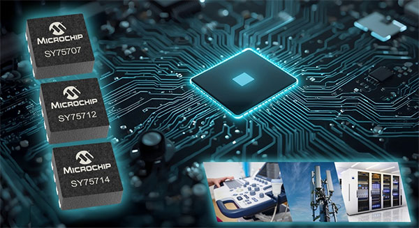
Microchip launches the SY757xx series 1.2V output LVCMOS clock buffer product portfolio to address the aforementioned design challenges. This series of devices does not require traditional discrete device solutions, simplifies system design, and provides ultra-low additional jitter performance. To support traditional board power design and clock sources of different voltage levels, this series of devices supports a wide range of power supply voltages (VDD) and a wide operating frequency range. The SY757xx series can achieve ultra-low additional jitter clock distribution while maintaining the high clock accuracy and signal integrity required for today's high-speed FPGA, SoC, and CPU platforms.
Maamoun Abou Seido, Vice President of Timing and Communication Business at Microchip, said, "With the development of next-generation high-performance FPGA, SoC, and CPU platforms, clock distribution is facing increasing challenges. Microchip's SY757xx clock buffer can help customers address these challenges. This single-chip solution integrates ultra-low additional jitter performance, wide range VDD support, and wide operating frequency support, which can simplify circuit board design, reduce device count, and help customers meet the signal integrity and timing accuracy requirements of today's high-performance computing applications. ”
In application platforms where signal integrity is crucial, the Microchip SY757xx series further strengthens the important role of clock buffers as SoC and FPGA clock distribution and fan out interfaces. These platforms need to support high-speed parallel processing, hardware reconfigurability, low latency, and efficient real-time computing capabilities. The above capabilities are widely applied in fields such as embedded vision, video processing, AI/ML acceleration, industrial control and IoT, network and communication, signal processing, and embedded systems.
This series includes 3 mass-produced devices and 8 devices currently undergoing small batch sample delivery, offering multiple configuration options and adopting 3 compact packaging forms. The device can suppress clock signal distortion in the frequency range of 0 Hz to 250 MHz, while supporting a voltage conversion input range of 1.2V to 3.3V, and providing rich power input and output options. Among them, the single-chip solution can achieve stable interconnection between 3.3V devices and FPGA and SoC that require 1.2V clock signals, with additional jitter as low as 26 femtoseconds (fs).
Compared with traditional discrete device solutions for FPGA and SoC applications, Microchip clock buffers can simplify design, reduce bill of materials costs, optimize AC coupling and bias circuits, and maintain signal integrity. The voltage divider circuit based on discrete devices may not provide sufficient design margin and may also reduce signal integrity due to duty cycle distortion.
Microchip clock buffers can be used in conjunction with the company's full range of flash based FPGAs and SoC FPGAs (from very low density to medium density). Microchip microcontrollers, analog devices, power management, timing, connectivity, and storage products have been pre designed and validated to help customers achieve simplified, low-risk, and more integrated system designs.
Supply and Pricing
The SY75707TWL-TR, SY75712TWL-TR, and SY75714TWL-TR devices in the low-power LVCMOS clock buffer series have now been mass-produced. SY75707TWL-TR supports differential input to two LVCMOS outputs and adopts an 8-pin ultra-thin dual flat no pin (VDFN) package. The SY75712 TWL-TR and SY75714 TWL-TR devices support 2 and 4 channels of 1.2V to 1.8V rail voltage LVCMOS outputs, respectively, and are packaged in an 8-pin thin dual row flat no pin (TDFN) package. Under a purchase quantity of 10000 pieces, the price range for a single piece is between $0.50 and $0.83, depending on the device configuration.
The remaining 8 SY757xx series devices support multiple types of inputs: single ended 1.2V to 3.3V LVCMOS input, single ended 1.2V to 1.8V LVCMOS input, differential 1.8V to 3.3V input, with outputs ranging from 1.2V to 1.8V LVCMOS levels; We also offer fan out buffer options with output enable (OE) functionality. All sample devices are packaged in 8-pin VDFN.
For more information and procurement, please contact Microchip sales representatives, authorized global distributors, or visit Microchip's procurement and customer service website at www.microchipdirect.com. If you need to obtain information about SY757xx samples, please send an email to tcghelp@microchip.com .


 Karmin Electronic (HK) Limited
  Hong Kong Tel:852-39070580 96557277
 Hong Kong Fax:852-39070581
 Email:
 Hong Kong address: Room 6, 11th floor, Huali industrial center, 10 - 14guidi street, Fo Tan, New Territories, Hong Kong