Samsung plans to build an advanced packaging plant in the United States with an additional investment of 7 billion US dollars!
2025-07-31
According to the Korean Economic Daily (Hankyung), Samsung is preparing to invest an additional $7 billion in the United States to establish an advanced semiconductor packaging factory after reaching a $16.5 billion chip foundry contract with Tesla.
According to reports, Samsung Chairman Lee Jae yong is expected to visit the United States soon to participate in ongoing trade negotiations. Therefore, this South Korean giant is expected to officially announce its plan to increase investment in the United States during or after the negotiations. It is expected that this investment will also become a bargaining chip for South Korea to play an active role in reaching a tariff agreement with the United States.
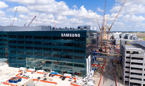
Samsung announced as early as 2021 the construction of a 5nm wafer fab in Taylor, Texas, USA. Although facing challenges such as local inflation, rising labor and material costs, the investment amount of the wafer fab has increased to 17 billion yuan, and the overall progress has continued to be delayed.
In April of this year, The Wall Street Journal reported that Samsung plans to build a new advanced process wafer fab, an advanced packaging plant, and a research and development center on top of its previously announced $17 billion investment in the United States, bringing the total investment amount to approximately $44 billion. However, the latest news suggests that due to the economic slowdown and a lack of customers, this investment has been reduced by billions of dollars.
However, with Samsung successfully winning Tesla's $16.5 billion chip foundry contract, it greatly enhances Samsung's confidence in continuing to invest in the United States.
Samsung Electronics announced in the relevant documents submitted on Monday that it has signed a chip foundry contract worth $16.5 billion, which is equivalent to 7.6% of Samsung's 2024 revenue. Samsung stated that the contract will take effect on July 24th and be valid until December 31st, 2033. Although Samsung has not disclosed the specific customer name, industry insiders speculate that the customer is likely to be Tesla, a US electric vehicle manufacturer. Subsequently, Tesla CEO Musk also confirmed this news.
Therefore, Samsung is expected to accelerate the mass production of its wafer fab located in Taylor, Texas, USA. Meanwhile, in order to complete the main manufacturing processes locally, Samsung plans to invest an additional $7 billion in the United States to establish an advanced semiconductor packaging factory.
As there are currently no high-end advanced packaging factories in the United States, TSMC's plan to build advanced packaging in the United States is expected to wait until around 2029 before mass production can begin. Therefore, for Samsung, establishing an advanced packaging plant in the United States as soon as possible will help enhance its competitiveness in the US wafer foundry market and better compete with TSMC.
The Korea Economic Daily also pointed out that Samsung is not the only South Korean company expected to invest billions of dollars in the United States. SK Hynix also plans to establish advanced DRAM factories in the United States for HBM production to meet the needs of major customers such as Nvidia. These investments are part of the South Korean delegation's efforts to ensure a better agreement with the United States, and it is expected that both sides will soon reach effective conclusions.


 Karmin Electronic (HK) Limited
  Hong Kong Tel:852-39070580 96557277
 Hong Kong Fax:852-39070581
 Email:
 Hong Kong address: Room 6, 11th floor, Huali industrial center, 10 - 14guidi street, Fo Tan, New Territories, Hong Kong