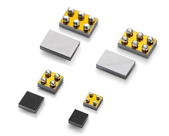
Litteluse launches a series of ultra-low power load switch integrated circuits to extend battery life
2023-12-22
Small size and first-class efficiency make it an ideal choice for IoT, mobile, and wearable electronic products.
Litteluse Corporation (NASDAQ: LFUS) is an industrial technology manufacturing company committed to providing power for sustainable development, interconnectivity, and building a safer world. It has announced the latest release of five multifunctional load switching devices in its protection integrated circuit product line.

These new load switch integrated circuits are ultra efficient load switches with rated currents of 2 and 4A, integrating true reverse current blocking (TRCB) and voltage swing rate control functions. Its first-class efficiency makes it an ideal choice for mobile and wearable consumer electronics products. These switches support the industry's lowest static current (IQ), low ON, and turn off current (ISD), helping designers reduce parasitic leakage current, improve system efficiency, and extend the overall lifespan of the battery. Watch the video.
The latest load switch integrated circuits are very suitable for various electronic product designs, including:
·Handheld devices,
·Wearable devices,
·Internet of Things (IoT),
·SSD storage,
·Building automation, and
·Consumer electronics products.
"The new load switch integrated circuit series supports extending the battery life of mobile and wearable products by providing low-power and power-saving features," said Bernie Hsieh, Assistant Product Manager of Littelhouse's Protection Semiconductor Business Team. "The chip level appearance of its packaging saves space and integrates multiple functions, such as swing rate control, true reverse current blocking, and fast output discharge."
Compared to previous solutions, load switch integrated circuits have the following main advantages:
·Energy saving can significantly extend battery life.
·Lower power consumption (lower RON, IQ, and ISD) provides efficient operation.
·These products use chip level packaging (using WLCSP) to replace discrete circuits with multiple functional integrations, such as power MOSFETs, reverse diodes, discharge MOSFETs, passive components, etc.
·The appearance of chip level dimensions also significantly reduces PCB space requirements.
There are several series of load switch integrated circuits:
·LQ05021QCS4-5V, 2A ultra-low power consumption, with slew rate control function
·LQ05021RCS4-5V, 2A ultra-low power consumption, with true reverse current blocking function
·LQ05022QCS4-5V, 2A ultra-low power consumption, with slew rate control function
·LQ05041QCS6-5V, 4A ultra-low power consumption, with slew rate control function
·LQ05041RCS6-5V, 4A ultra-low power consumption, with true reverse current blocking function
The load switch device adopts a small chip level packaging, which has:
·Four (4) protrusions, package size 0.77mm x 0.77mm x 0.46mm, with a spacing of 0.4mm,
·Four (4) protrusions, chip size 0.97mm x 0.97mm x 0.55mm, with a spacing of 0.4mm, or
·Six (6) protrusions, package size 0.97mm x 1.47mm x 0.55mm, with a spacing of 0.5mm.

